Semiconductor Co., Ltdwas founded in 2019, which is located at Zhangjiagang, the national civilized and healthy city. The company’s address is No. 2 Fuxin Road, High-tech Development Zone, Zhangjiagang City, with 480 million yuan of total one-phase investment, covering an area of 55 mu,and 71,000 square meters of construction area, where its super clean room area is 6,000 square meters and supporting facilities of factory are 3,000 square meters.
Total one-phase investment of 480 million yuan
Covering an area of 55mu
construction area of 71000㎡
Super clean room area6000㎡
Factory facilities3000㎡
The company mainly undertakes the service such as the development of semi-conductor process technology, technical consultation, technical transfer and its related technical service; Semiconductor separation device, semiconductor lighting device, power electronic component manufacturing, gallium port, sales; new materials, semiconductor separation device testing services; the training service facing to adults(not including the national unified recognition of vocational certificate training); information technology services.

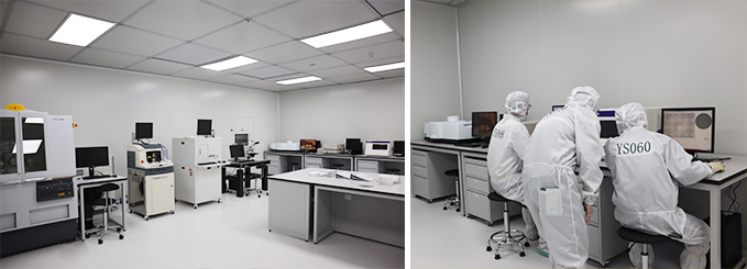
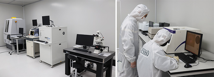
The company has owned completed epitaxial production line, which includes 3 sets of MOCVD12×6”equipment production machine, one set of MOCVD6×2”research and small batch of production machine for producing HBT, pHEMT, VESEL and detectors of gallium arsenide and indium phosphide, matched with a complete epitaxial inspection service platform,which can realize the test and analysis of surface particle size, square resistance, mobility and material structure of epitaxial wafer and meanwhile it will be open to outside for authorized use, adhering to principle of serving scientific research and society.
Company Aims
Jiagang Semiconductor CO.,LTD insists in satisfying national strategic needs and promoting the development of economic society, and besides, in accordance with the industrial deployment and actual demands in Zhangjiagang City, it focuses on the nanometer materials, power electronics, laser communication, and photo sensor these cutting-edge technologies, and key semiconductor components urgently needed to be solved by the country, devotes to key technological breakthrough in the field of compound semiconductor with GaAs, InP, GaN, and SiC as representatives, extension technology service, construction of public testing platform, talent project introduction, and industrialization, and tries to take the lead in creating the platform for the transformation of scientific and technological achievements for integrated innovation of political research.